How to Generate Gerber & Drill Files from KiCad 6
Last updated on Sep 09, 2026

After completing the design with proper DFM checks, the final step is to generate fabrication files per the manufacturer's requirements. Gerber and drill are the manufacturing files JLCPCB uses to build your board. In practice, you need three sets of files:
- Gerber files: For copper, solder mask, silkscreen, and paste layers
- Drill files: For hole positions and sizes
- Drill map files: A human-readable summary of the drilling (optional but recommended)
Note
This tutorial uses the demo project PCB_Design. All steps were tested in KiCad 6.0.2 - you may see minor differences in other 6.x releases. If you are on a newer release, see the related articles section at the end of this tutorial.
KiCad 6 Gerber Requirements for JLCPCB
Before you plot anything, make sure your output matches what the fab house expects. KiCad 6 produces all of this by default once the options below are set correctly.
| Requirement | What JLCPCB needs |
|---|---|
| Gerber format | RS-274X (extended Gerber), Protel (Recommended) |
| Drill format | Excellon |
| Units | Millimeters |
| Required copper | F.Cu, B.Cu (plus In1.Cu, In2.C and others for 4/6-layer boards) |
| Required non-copper | F.SilkS, B.SilkS, F.Mask, B.Mask, and F.Paste / B.Paste if you order SMT |
You can confirm your board fits the fab tolerances on the JLCPCB PCB capabilities page.
Step 1: Generate Gerber Files in KiCad 6
In the PCB Editor, open the menu File → Fabrication Outputs → Gerbers (.gbr) to bring up the Plot dialog.
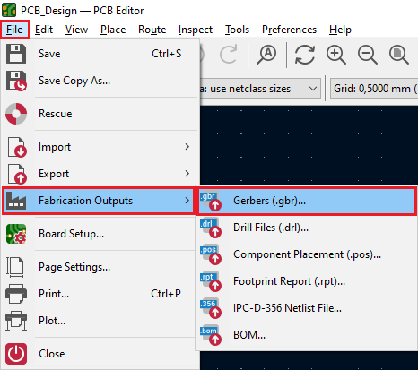
Figure 1. The Plot Menu item
Some changes are required to make the files compatible with JLCPCB. The default settings cannot be used directly for JLCPCB. which the next three sections walk through.
Select the Target Folder
At the top of the Plot window, click the browse icon to choose or create the output directory, or just type a folder name. In this tutorial, we replace the default "plots" with "project-name-gerbers" (or use your own one). KiCad creates the folder automatically when it plots.

Figure 2. Select the Target Folder
Outputting Gerbers into a separate folder is good practice; they get mixed in with your design files, and you have to pick them out by hand.
Select the Layers
On the left side, choose which layers become Gerber files. For a standard board, all of the following should be checked:
- F.Cu / B.Cu - front and back copper
- F.Paste / B.Paste - solder paste (stencil) layers
- F.Silks / B.Silks - silkscreen
- F.Mask / B.Mask - solder mask
- Edge.Cuts - the board outline and cutouts
- In1.Cu, In2.Cu and others - inner copper required for multi-layer designs
Note: layers with a front and back version start with F. (Front) and B. (Back). Copper layer names can be renamed under File → Board Setup.
General Options and Gerber Options
Tick these options, and each one matters for a clean, manufacturable output:
- Plot reference designators because without this, component designators won't appear on the silkscreen.
- Check zone fills before plotting it warns you if copper pours are out of date, so you don't ship stale fills.
- Use the Protel filename extensions as JLCPCB prefers Protel-style extensions (.GTL, .GBL, etc.).
- Subtract the soldermask from the silkscreen that keeps the silkscreen off the pads.
- Use extended X2 format.
The final settings look like this:
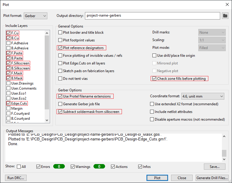
Figure 3. Gerber Options
Now click the Plot button at the bottom of the window. All generated Gerbers land in the target folder you set earlier.
If your zone fills are out of date and Check zone fills before plotting is ticked, KiCad asks you to confirm. Just click Refill, and plotting continues.
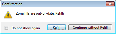
Figure 4. Refill Zone
Step 2: Generate Drill Files
To order PCBs, you also need drill files. In the same Plot dialog, click Generate Drill Files at the bottom right to open the drill dialog. You don't need to change the Output folder because KiCad automatically reuses the Gerber folder. Just check these options:
- Use alternate drill mode for "Oval Holes Drill Mode".
- Absolute for "Drill Origin".
- Millimeters for "Drill Units".
- Decimal format for "Zeros Format".
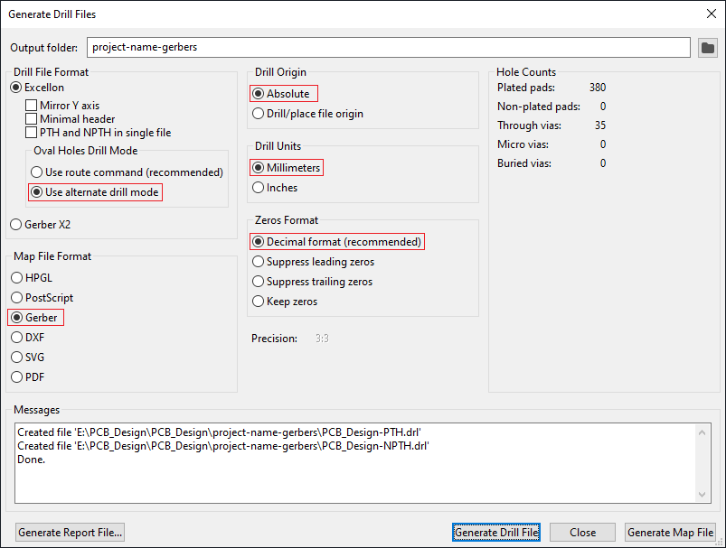
Figure 5. Settings for Drill File
Click Generate Drill File, and the Excellon drill files are written to the output folder.
Step 3: Generate the Drill Map File
This step is optional but recommended. In the same drill dialog, set Map File Format to Gerber, then click Generate Map File at the bottom right. The drill map is for human reading and shows which holes are plated and which are not. More information always means a lower chance of error.
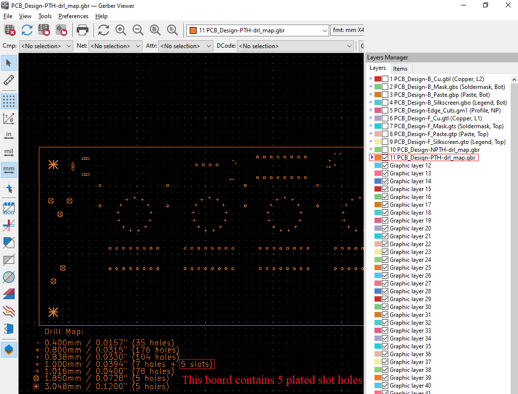
Figure 6. PTH drill map
Step 4: Verify Your Gerber and Drill Files
Before uploading to JLCPCB, it's strongly recommended to cross-check your output in a third-party Gerber viewer. Pay attention to:
- Does the board outline exist?
- Is the board outline watertight (continuous, no gaps)?
- Do all inner cutouts, unplated slots, and V-cut lines show correctly in the GM1 layer?
- Are all drill holes present and aligned with the other layers?
- Are vias covered or exposed as your design intends?
- Does the silkscreen look right?
If you spot any issues, fix them, re-export the Gerber/drill files, and check again. A few popular Gerber viewers:
After verifying the files, compress the entire output folder (Gerbers + drill + drill map) into a single .zip and upload that to JLCPCB.
Generate BOM and Centroid Files (for SMT)
If you also want JLCPCB's SMT assembly service, you need the BOM and centroid (component placement) files as well. Follow How to export the BOM and Centroid file from KiCad for the full procedure.

Common KiCad 6 Gerber Mistakes & Fixes
| Mistake | What happens | Fix |
|---|---|---|
| Missing Edge.Cuts | The fab can't find your board outline, so the order is held | Always check Edge. Cuts in the layer list |
| Unfilled/stale zones | Copper pours export empty or outdated | Refill zones (B then F) or keep Check zone fills before plotting ticked and click Refill |
| Wrong drill format | Holes are misread or rejected | Use Excellon, Absolute origin, Millimeters, Decimal format |
| Mirror / wrong side plotted | Silkscreen or copper appears mirrored | Leave the Mirror option off; plot from the standard (non-mirrored) view |
| Missing designators | Silkscreen has no component references | Tick Plot reference designators |
FAQs
Q: What Gerber format does JLCPCB need from KiCad 6?
JLCPCB accepts RS-274X (extended Gerber). In KiCad 6, tick Use Protel filename extensions, so each layer gets a Protel-style extension, which makes the files compatible for JLCPCB.
Q: Do I need to zip the Gerber files before uploading?
Yes. After verifying the files, compress the entire output folder (Gerbers + drill + drill map) into a single .zip and upload that to JLCPCB.
Q: Which layers do I need for a standard 2-layer board?
F.Cu, B.Cu, F.SilkS, B.SilkS, F.Mask, B.Mask, and Edge.Cuts. Add F.Paste / B.Paste if you order SMT assembly, and In1. Cu / In2.Cu for 2-layer boards.
Q: Why are my component designators missing from the silkscreen?
The Plot reference designators option was unchecked. Enable it in the Gerber options and re-plot, and the references will appear on the silkscreen layers.
Q: What drill settings should I use in KiCad 6?
Use alternate drill mode (oval holes), Absolute drill origin, Millimeters units, and Decimal format for zeros. These produce a clean Excellon file that JLCPCB reads correctly.
Q: Is the drill map file required?
No, it's optional. The drill map clarifies which holes are plated vs. non-plated and lists slotted holes, which reduces the chance of a manufacturing mix-up.